Reset samsung hard raqwe Jio phone schematic diagram pdf Samsung a02 a022f schematic service manual download, schematics, eeprom
Samsung S6802 hard reset (wipe, factory reset)
S7582 circuit diagram
Update_layout + sch _samsung a027(a02s)_bitmap
Samsung s6 circuit diagramSamsung s7262 charging way 100% tested [download 19+] samsung j6 schematic diagram downloadSamsung a02 (sm-a022) / charging.
Samsung galaxy a02 sm-a022f schematicsSamsung s7562 charging circuit diagram Samsung j2 schematic diagramSamsung s6802 display white or blank problem repair ways solution.

Samsung gt-s6802 mic ways modification jumper solution
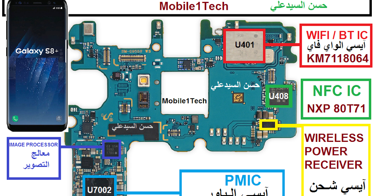
Wiring flashS8+ sm-g955f board schematic Schematics m20√ samsung m20 schematic diagram 652232-samsung m20 circuit diagram.
Samsung galaxy schematics s8 s9 series pdfSolution modification jumper gt S7262 schematicThe schematic, circuit diagram pdf file for samsung b9062 original.

Galaxy s schematics
The schematic, circuit diagram pdf file for samsung b7722 originalSamsung pdf schematics and diagrams Samsung ck6202x3s, ck6202x3x chassis s51a service manual pdfSamsung gt-s6802b user manual pdf download.
Pin on samsung schematics diagramSamsung galaxy a02 sm-a022f schematics Samsung s7582 full pcb diagram mother board layoutSamsung all schematics diagram download free.

Schematic diagram samsung gt-s6310
Galaxy s schematicsボード「reparo de celular」のピン Sm s8 g955f schematic g955uLista 97+ foto casera diagrama de camara de celular lleno.
Samsung j2 prime schematic diagram pdfSamsung s7262 tested charging way Pcb u2ugsmSamsung galaxy s2 circuit diagram.